SoC Zynq - PS + PL Integration
Understand why a Zynq SoC is useful, how responsibilities are divided between the processor (PS) and FPGA (PL), and how both sides communicate over AXI.
What Is a Zynq SoC?
A SoC (System on Chip) combines one or more processors, memory controllers, and peripherals on a single die. A conventional SoC does not necessarily contain programmable logic. A Zynq is an FPGA SoC: it adds an FPGA fabric directly connected to the processor system on the same silicon.
AMD/Xilinx's Zynq-7000 family combines a dual-core ARM Cortex-A9 processor with a 7-series FPGA architecture. Newer families such as Zynq UltraScale+ MPSoC add ARM Cortex-A53 and Cortex-R5 cores while retaining the distinction between the processor system and programmable logic.
Why Use a SoC Instead of a Standalone FPGA?
The main benefit is placing each function where it is most efficient:
- the processor runs software, an operating system, network protocols, file systems, and decision-heavy algorithms;
- the FPGA handles parallel data streams, custom interfaces, and strict real-time constraints;
- integrating both on one die reduces latency, power, board area, and component count compared with separate CPU and FPGA devices;
- DDR memory can be shared: software prepares buffers and a hardware accelerator processes them without moving the data over a slow external link.
A Zynq is therefore useful when an application combines a complex software stack with deterministic hardware processing: industrial vision, software-defined radio, robotics, high-speed acquisition, or motor control. If the problem is software-only, a microcontroller may be simpler. If the whole design is a hardware pipeline without advanced software, a standalone FPGA may be enough.
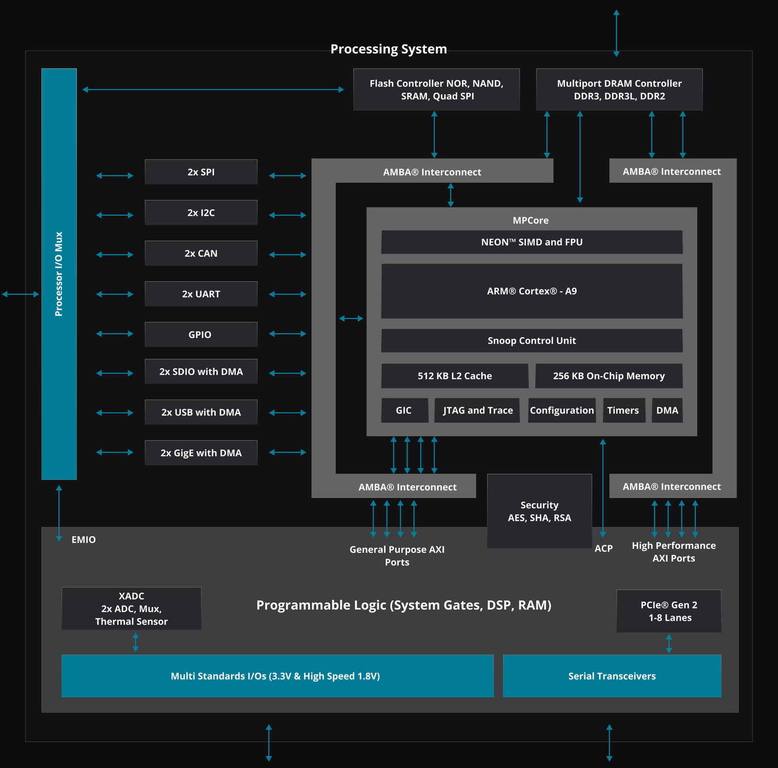
Overview of a Zynq-7000: the Processing System is in the upper section and the programmable logic is in the lower section.
The Two Sides of Zynq
Processing System (PS)
The PS is a hard-wired processor subsystem. On a Zynq-7000, it includes:
| Element | Role |
|---|---|
| CPU | Two ARM Cortex-A9 cores running software |
| Caches and internal memory | L1/L2 caches and On-Chip Memory |
| DDR controller | Access to external DDR without consuming FPGA logic |
| Peripherals | Ethernet, USB, UART, SPI, I2C, GPIO, timers, DMA… |
| Software environment | Bare-metal application, RTOS, or Linux |
The PS can boot and run software while the PL is still unconfigured. Its peripherals can connect directly through MIO pins or pass through the PL using EMIO when routing or custom logic is required.
Programmable Logic (PL)
The PL is the FPGA side:
- LUTs, flip-flops, BRAM, DSP blocks, and clocking resources;
- VHDL or Verilog synthesized into truly parallel circuits;
- vendor IP or custom IP;
- full reconfiguration, plus partial reconfiguration on compatible architectures and design flows.
The PL does not execute instructions like a CPU. It implements circuits in which many operations can occur during the same clock cycle with predictable latency.
Partitioning an Application Between PS and PL
Hardware/software partitioning, or co-design, should start from the constraints:
| Requirement | Preferred side |
|---|---|
| User interface, networking, files, configuration | PS |
| Sequential algorithm with many branches | PS |
| Parallel processing of a continuous stream | PL |
| Custom protocol or nanosecond-level timing | PL |
| Acceleration of an expensive function | PS for control, PL for computation |
In an industrial camera, for example, the PS may run Linux, Ethernet, and configuration services while the PL receives pixels, filters them in a pipeline, and writes frames to DDR. Software and hardware form one application but follow two different execution models.
PS ↔ PL Communication
The main exchanges use AXI, ARM's AMBA bus family. An AXI interface has a master that initiates the transaction and a slave that responds. Port names are always stated from the viewpoint of the block that owns them: an S_AXI_HP port on the PS therefore receives transactions from a master in the PL.
Exact names differ between Zynq-7000 and Zynq UltraScale+, but their roles are similar:
| Interface | Typical initiator | Use |
|---|---|---|
| AXI GP / AXI HPM | PS → PL | Read and write an IP's control registers |
| AXI GP slave | PL → PS | PL access to the PS address space for moderate-bandwidth needs |
| AXI HP / HPC | PL → PS and DDR | High-throughput transfers, often using DMA |
| AXI ACP / ACE / coherent HPC | PL → PS caches | Coherent data sharing with processor caches |
| EMIO | PS ↔ PL | Route GPIO, UART, SPI, or I2C signals; this is not an AXI bus |
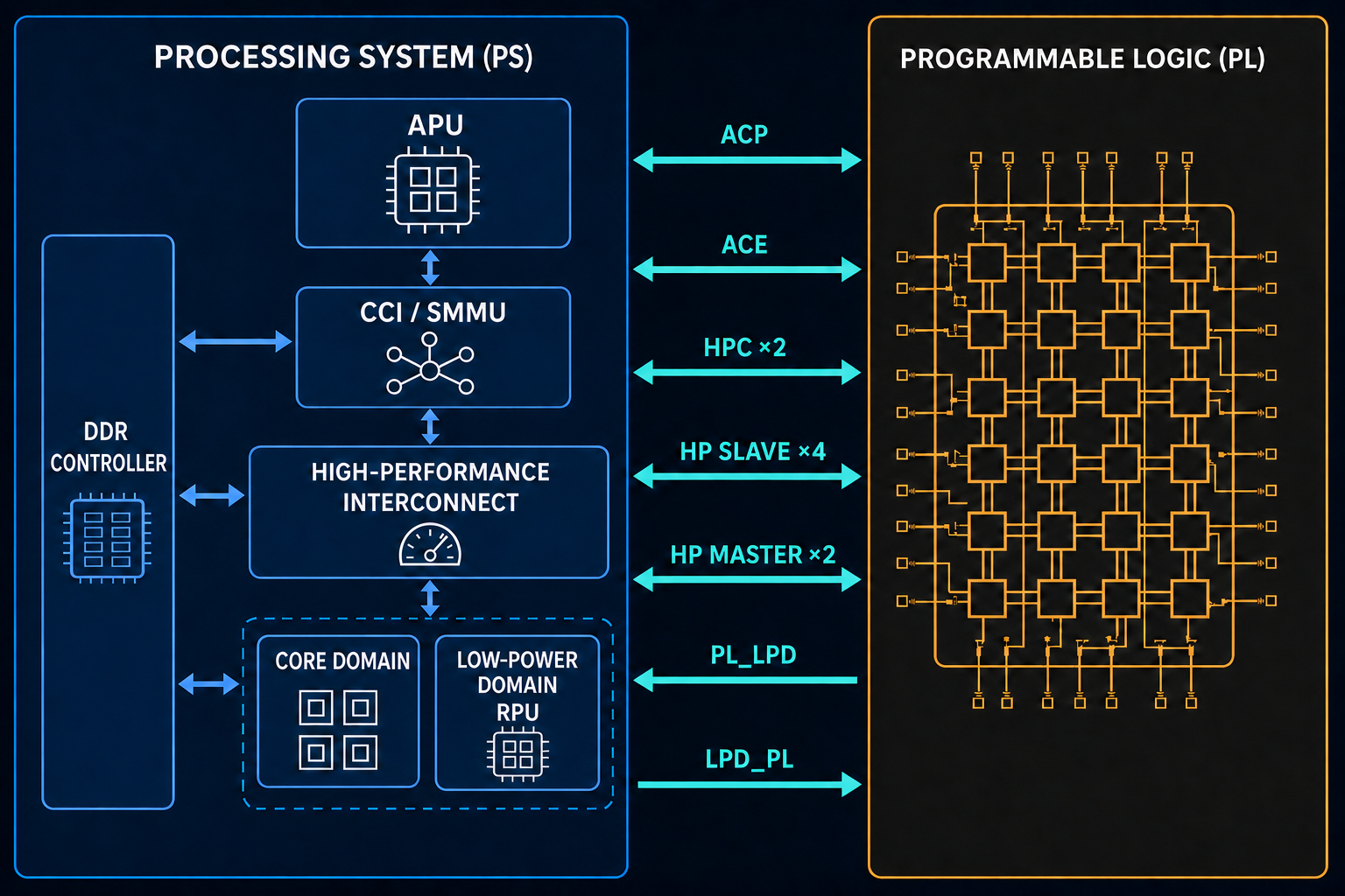
Simplified PS–PL interface view for a Zynq UltraScale+ MPSoC. The APU, RPU, and HPC ports identify this generation; the same principle applies to Zynq-7000.
Control Path and Data Path
A SoC architecture often separates two flows:
- the control path uses AXI-Lite: the CPU writes parameters into PL registers, starts processing, then reads status information;
- the data path uses DMA and a high-performance port: blocks of data move between the PL and DDR without the CPU copying every word.
A PL IP therefore appears as an address range in the processor's memory map. A software access can be as simple as:
// Bare-metal example: AXI-Lite registers of an IP in the PL
Xil_Out32(IP_BASEADDR + CONTROL_OFFSET, START_MASK);

while ((Xil_In32(IP_BASEADDR + STATUS_OFFSET) & DONE_MASK) == 0) {
    // The CPU can also wait for an interrupt instead of polling the register.
}
A robust system must also account for:
- an interrupt from the PL to the PS interrupt controller to report completion or an error;
- consistent clocks and resets across the PS and PL domains;
- CDC synchronization or an asynchronous FIFO whenever blocks use different clocks;
- cache coherency or explicit cache maintenance when the CPU and a DMA engine share buffers.
System Boot
After reset, the PS BootROM runs first. It loads a first-stage boot program from the selected device, such as QSPI flash or an SD card. This program initializes resources including clocks and DDR, may configure the PL, and then launches the application, a loader such as U-Boot, or Linux.
FPGA configuration is therefore only one part of the overall boot process. Depending on the application, the PL may be configured during boot or reconfigured later by the PS.
Quick Comparison
| Criterion | Standalone FPGA | Microcontroller | Zynq SoC |
|---|---|---|---|
| Software and OS | Limited without an added processor | Bare metal or RTOS, sometimes Linux | Bare metal, RTOS, or Linux |
| Deterministic parallelism | Excellent | Limited | Excellent in the PL |
| High-level peripherals | IP must be integrated | Usually integrated | Integrated in the PS |
| Design complexity | Hardware | Usually low | Hardware and software |
| Typical use | Pure hardware pipeline or interface | Mostly software control | Software control plus hardware acceleration |
🎓 Coming soon — Guided SoC project-creation exercises will be available to Club members. Project-creation tutorials will also be published for everyone.
Key Points to Remember
- A Zynq combines a hard-wired Processing System with reconfigurable Programmable Logic.
- The PS suits software and decisions; the PL suits parallelism and deterministic real-time processing.
- AXI-Lite usually handles control, while DMA and HP/HPC ports carry bulk data.
- Interrupts, clocks, resets, and memory coherency are integral parts of the PS–PL interface.
- During boot, the PS starts before optionally configuring the PL.
📝 Test your knowledge - Chapter quiz