Block Design & IPs
Using Vivado block design and vendor IPs to build SoC-based FPGA designs.
What is Block Design?
Block design is an alternative way to develop on FPGA. Instead of writing VHDL, you can visually assemble IPs (Intellectual Properties) - functional blocks provided by the vendor or created yourself - and connect them graphically.
Key advantages:
- Connect proprietary protocols (AXI, etc.) easily and visually
- Use vendor-optimized IPs (memories, processors, controllers)
- Simplify connections between blocks in SoC designs
Block designs are especially useful when working with a SoC. To use the CPU, you rely on vendor-provided blocks to communicate with memories and the processor from the FPGA fabric.
Step-by-step Tutorial - ZYNQ Z2
The tutorial uses a simple example: blink LEDs using push buttons on a ZYNQ Z2 board.
This will demonstrate:
- How to use IPs
- How a SoC board works
Step 1 & 2 - Create the Vivado Project
Create your Vivado project and select your target board. Refer to the First Vivado Project course if needed.
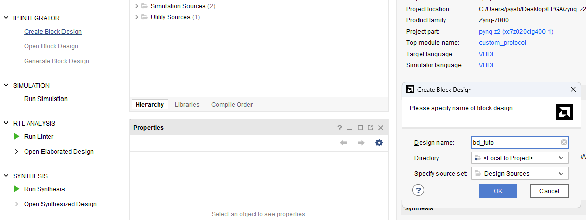
Step 3 - Create the Block Design
Click "Create block design" and give it a name (e.g. bd).
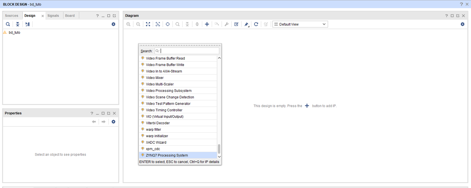
Step 4 - Add the Processing System
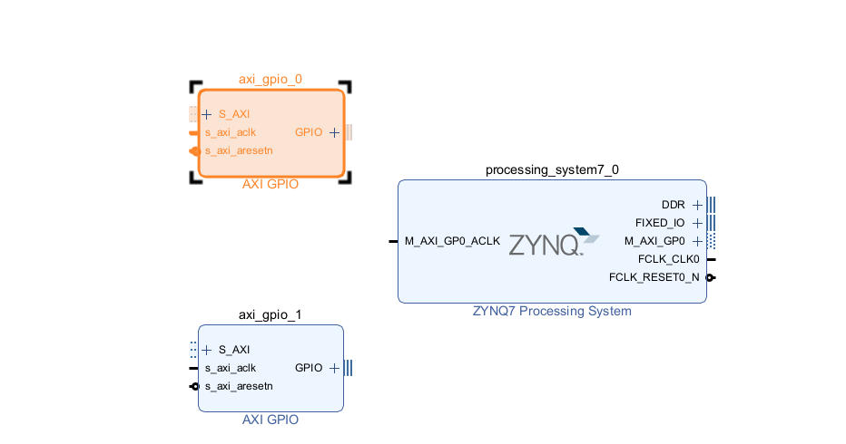
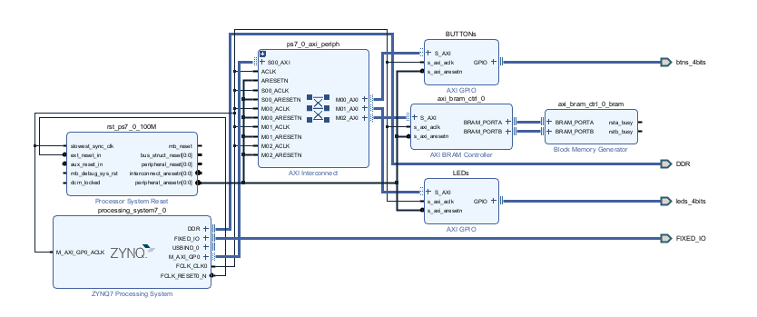
You arrive on a page where you can add IPs. Search for and add the Processing System matching your board (Zynq7 Processing System for the ZYNQ Z2).
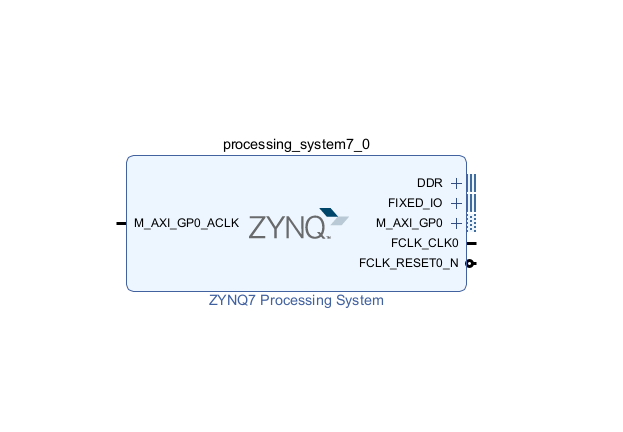
You should get this result:
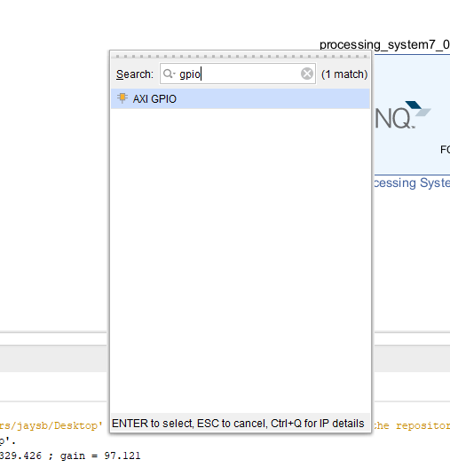
Step 5 - Add GPIO IPs
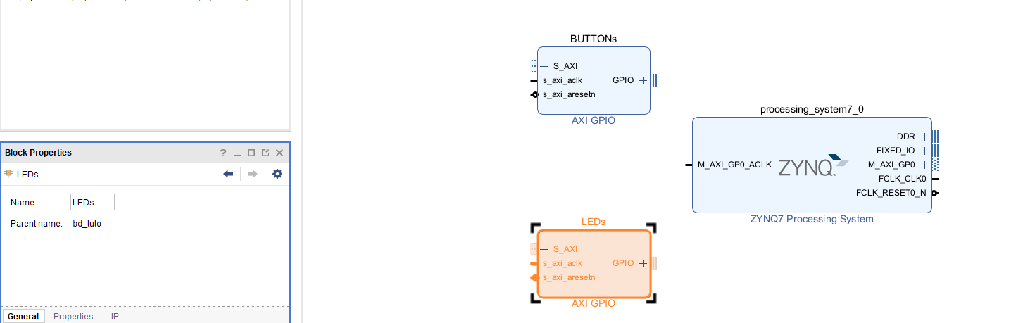
Right-click → Add IP and search for GPIO. Add two instances: one for LEDs, one for buttons.
In the Block Properties tab, rename the blocks LEDs and BUTTONs for clarity.
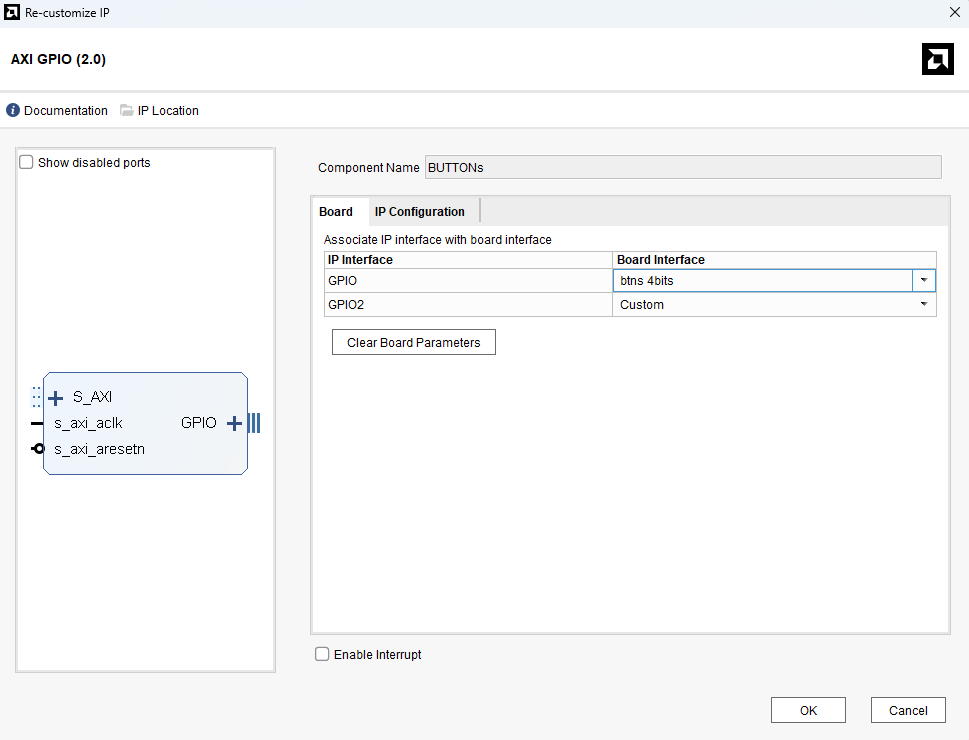
Configure the I/O of each block. For BUTTONs, select btns_4bits. Feel free to delete auto-generated outputs and rerun "Run Connection Automation".
Step 6 - Automatic Connection
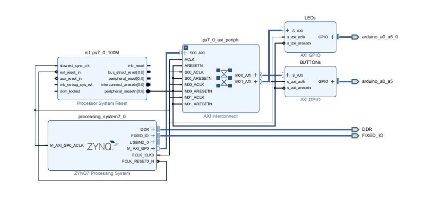
Click "Run Block Automation" then "Run Connection Automation" and select all. Vivado will automatically connect the blocks.
Step 7 - Add an AXI BRAM
To allow the CPU to access the LEDs and buttons, it needs an AXI memory. Add an AXI BRAM Controller IP and redo step 6.
Step 8 - Create Your Own IP
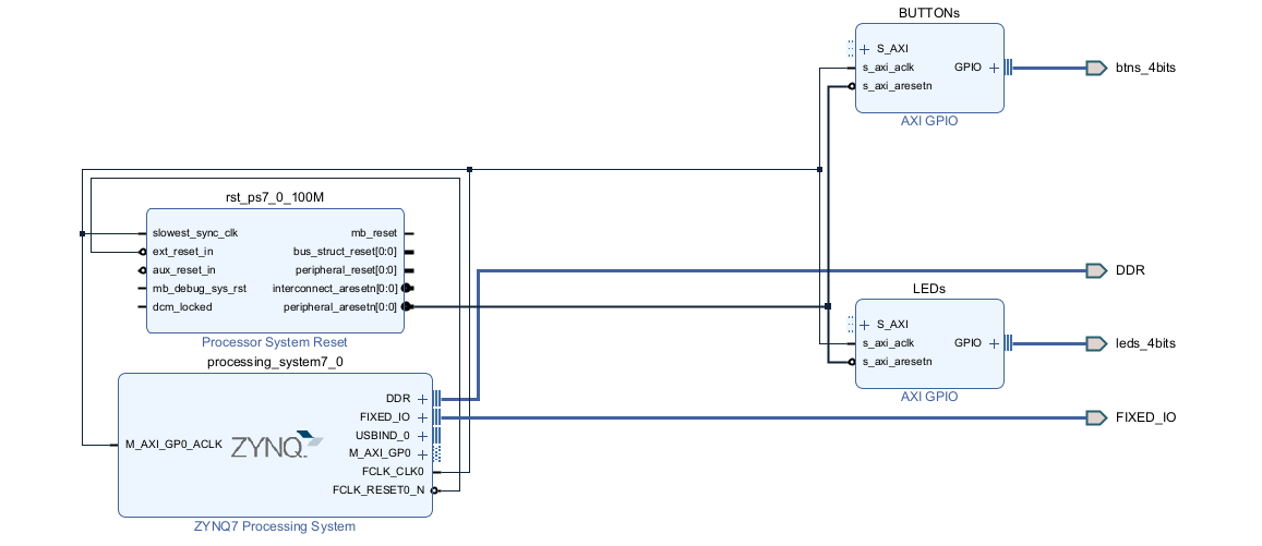
Our final goal is to create a custom IP to connect LEDs directly to buttons. Clean up the design first.
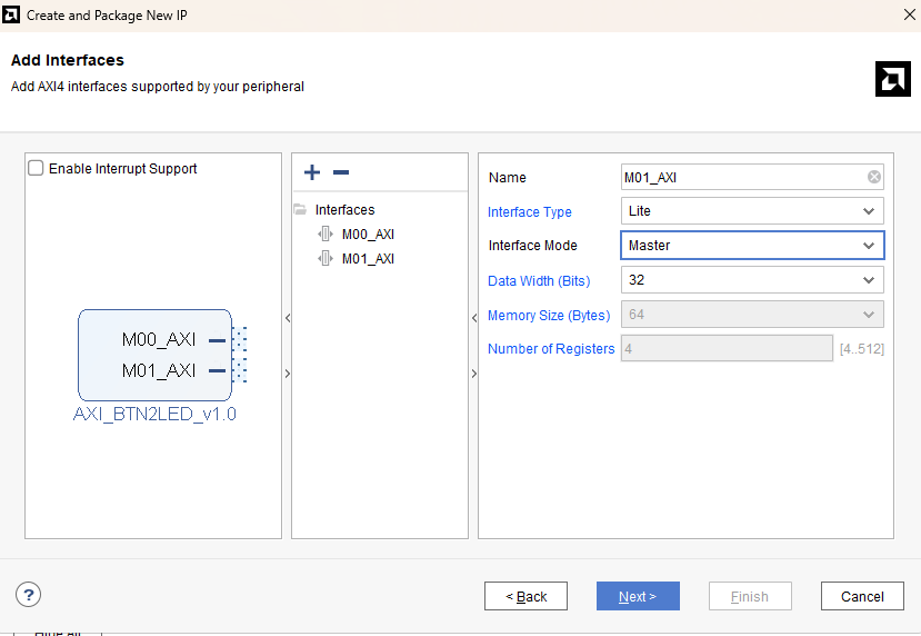
Step 9 & 10 - Create and Package the IP
Go to Tools → Create and Package new IP. Choose an AXI-Lite Master interface (same as AXI GPIO). Add two instances: one for LEDs, one for buttons. On the last page, click "Edit IP".
Summary
| Concept | Description |
|---|---|
| IP | Reusable functional block (vendor-provided or custom) |
| Processing System | The SoC CPU portion (Zynq) |
| AXI GPIO | IP for controlling GPIO over the AXI bus |
| AXI BRAM | Memory accessible by the CPU via AXI |
| Run Connection Automation | Vivado auto-connects compatible blocks |
To go further, understanding the AXI protocols is essential. See the AXI Protocol course.
📝 Test your knowledge - Chapter quiz